
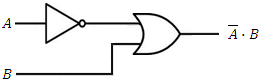
Examples of logical gates circuits
|
||||||||||||||||
|
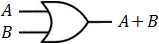
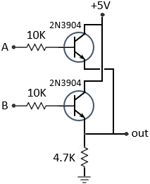
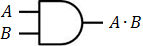
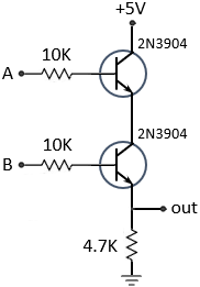
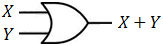
Logical gates are the basic of the computerized world and is based on the digital values of the binary
numbers 0 and 1. The implementation of the logical gates are performed by the rules of the
Boolean algebra, and based on the combinations of the operations OR, AND and NOT. The specific
gate operation is attained by using diodes or transistors that acts like a switch 0 is off
(0 Volt) and 1 is on (5 Volt).
|
||||||||||||||||
|
|||||||||||||||||||||||||||||||||||||||||||||||||||||||||||||||||||||||||||||||||||||||||||||||||
|
|||||||||||||||||||||||||||||||||||||||||||||||||||||||||||||||||||||||||||||||||||||||||||||||||


|
|||||||||||||||||||||||||||||||||||||||||||||||||||||||||||||||||||||||||||||||||||||||||||||||||||||||||||||||||||||||||||||||||||||||||||||||||||||||||||||||||||||||||||


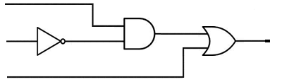
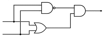
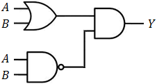
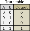
The truth table at points D, E, F, G, H and K of the system described above are.
|


|
||||||||||||||||||||||||||||||||||||||||||||||||||||||||||||||||||||||||||||||||||||||||||||||||||||||||||||||||||||||||||||||


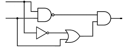
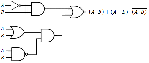
The truth table at points D, E, F, G, H, I, J, and K of the system described above are.
|


|
|||||||||||||||||||||||||||||||||||||||||||||||||||
|


 (D equals 1 see above)
|
||||||||||||||||||||||||||||||||||||||||||||||||||||||||||||||||||||||||||||||||||||||||||||||||||||||||
|


|
|||||||||||||||||||||||||
|
|||||||||||||||||||||||||
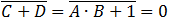
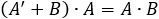
Order of evaluating Boolean expressions

From algebra we know that the order of calculating mathematical expressions are first powers and roots then multiply and divide
and at last addition and subtraction. The question now is what is the correct order of evaluating Boolean expressions.
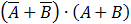
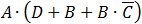
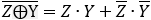
We can do first the NOT operation then the AND, and in the end the OR operation, but many times that order is not what we
need to do. check for example the following expression:  .
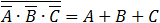
We calculated the expression in the bracket first. We can clearly see that the results are not the same. To prevent this
kind of problems it is highly recommend that we set the priority operations by brackets.
.
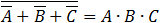
We calculated the expression in the bracket first. We can clearly see that the results are not the same. To prevent this
kind of problems it is highly recommend that we set the priority operations by brackets.

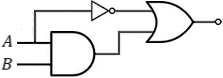
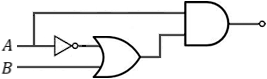
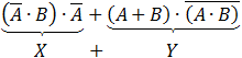
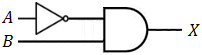
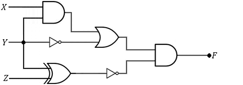
3D lines - Example 12
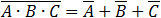
 . Draw the proper
logical gates circuit describing this expression then draw the truth table, finally simplify the expression.
. Draw the proper
logical gates circuit describing this expression then draw the truth table, finally simplify the expression.
The logical gates of the given equation will be as follows:


| Port | Value | Notes |
| A |  |
|
| B |  |
|
| C |  |
|
| D |  |
The order is:  |
| E |  |
|
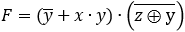
| F | ![[NOT (y) OR (x AND y)] AND NOT (z XOR y)](/MathCalc/LogicCalc/Examples/eq/ex12f.PNG) |
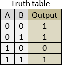
| X | Y | Z | A | B | C | D | E | F |
|---|---|---|---|---|---|---|---|---|
| 0 | 0 | 0 | 0 | 1 | 0 | 1 | 1 | 1 |
| 0 | 0 | 1 | 0 | 1 | 1 | 1 | 0 | 0 |
| 0 | 1 | 0 | 0 | 0 | 1 | 0 | 0 | 0 |
| 0 | 1 | 1 | 0 | 0 | 0 | 0 | 1 | 0 |
| 1 | 0 | 0 | 0 | 1 | 0 | 1 | 1 | 1 |
| 1 | 0 | 1 | 0 | 1 | 1 | 1 | 0 | 0 |
| 1 | 1 | 0 | 1 | 0 | 1 | 1 | 0 | 0 |
| 1 | 1 | 1 | 1 | 0 | 0 | 1 | 1 | 1 |
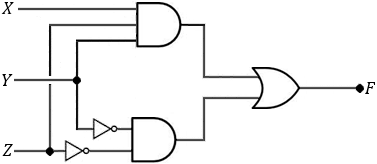

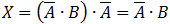
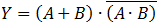
According to the Boolean algebra equations summary we get:

The first item is equal to 0 and finally we get the simple value which is equivalent to the given equation:

Now press the various buttons in the first circuit inputs to show that both outputs F are the same.