Logical gates are the basic of the computerized world and is based on the digital values of the binary
numbers 0 and 1. The implementation of the logical gates are performed by the rules of the
Boolean algebra, and based on the combinations of the operations OR, AND and NOT. The specific
gate operation is attained by using diodes or transistors that acts like a switch 0 is off
(0 Volt) and 1 is on (5 Volt).
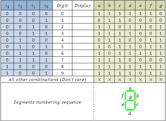
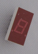
A seven-segment display is an electronic device for displaying decimal numbers. widely used for electronic clocks
and counters. The display is designed by using logical gates.
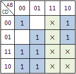
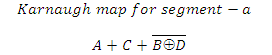
Each segment of the number can be calculated by using the Karnaugh method (see above).
Left shift is performed by moving all the bits one place to the left and filling 0 in the last place, most left bit is lost or moved to the next higher level.
For example, the byte 10011001 after left shift will be: 00110010
If we remember the most left bit, the left shift operation is equivalent to multiplying the number by 2. For example the byte 00001110 equals 14 decimal, after left shift we get 00011100 which is equal to 28.
Draw logical gate circuit from Boolean expression example 11
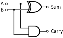
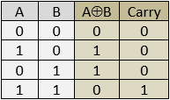
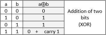
The half adder performs the addition of two bits with an XOR gate
and return a carry with an AND gate in case that both A and B are equal to 1.
The difference between Half Adder and Full Adder is the input of a
carry to the Full Adder, three inputs (see example 12a). After calculation they both return the sum and a carry.
The full adder adds the values of two bits A and B, if
both bits are equal to 1 then it passed through the value of the carry to the next calculation level.
For the first loop (rightmost bit) the input carry equals to 0. In order to add two bytes, we can add 8 full adders (see next example).
The basic circuit for adding two bits contains the chips IC 7486 - quad XOR gate, IC 7408 - quad AND gate and IC 7432 quad OR gate.
We used only half of the gates of the XOR and AND gates and only 1 of the OR gate. All the chips have to be connected to the input voltage at Vcc and to the ground at GND input.
The carry out values can be connected to the carry input of the next pair of bits and so on until we reach the number of bits that should be added, see next example for 4 bits addition, this case uses all the inputs of the three types of chips 7486, 7408 and 7432.
The 4 bits adder adds the values of two 4 bits values
and gives the result at right, notice that the result contains additional carry that can be used for the next higher calculations.
This process can be easily extended to more bits.
Example - Add the 4 bits binary number 1011 (decimal 11) to the binary number 0110 (decimal 6)..
Notice that in binary addition 0 + 0 = 0 0 + 1 = 1 1 + 1 = 0 and carry 1.
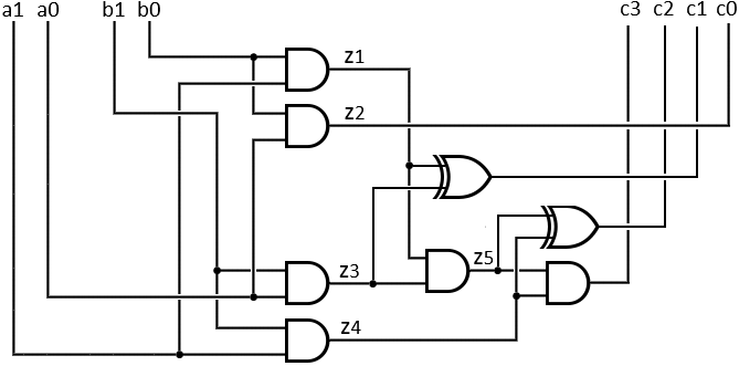
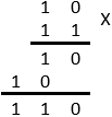
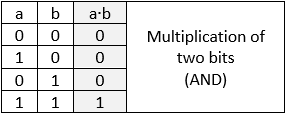
Let multiply two bits first bit is: (1 0) and the second bit is: (1 1) the result of this multiplication is:
The multiplication is made according to the following rules:
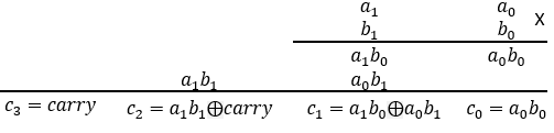
The general process of multiplying two sets of two bits (a1 a0) and (b1 b0) is according to the following steps:
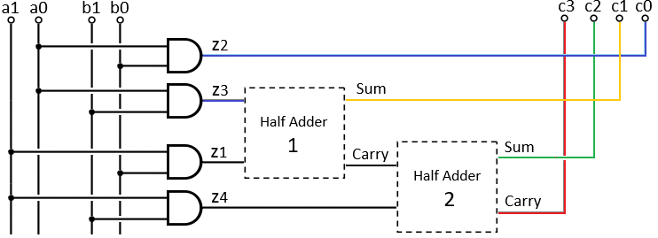
In order to better understand the circuit of the set of two, two bits multiplier we draw the circuit with
the half adder as a box, now we can see clearly way the calculations take place.
1) The result of the first multiplication is the value of c0 = a0b0 (blue line).
2) Now perform the addition of c1 = a1 b0 ⨁ a0 b1.
This operation is performed by the half adder no. 1 circuit because it gets two values which are not including a carry from c0.
(see example 12). The result sum is the value of c1 (yellow line).
3) Now perform the addition of c2 = a1 b1 ⨁ carry.
This operation is performed by the half adder no. 2 circuit notice that one input is the result of the carry from half adder number 1.
The sum is the value of c2 (green line).
4) The result of the carry of the second adder is the value of c3 (red line).


 (D equals 1 see above)